Abstract
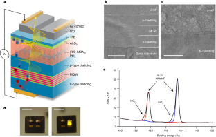
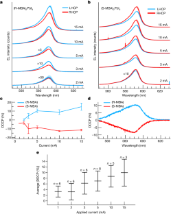
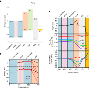
Spin accumulation in semiconductor structures at room temperature and without magnetic fields is key to enable a broader range of optoelectronic functionality1. Current efforts are limited owing to inherent inefficiencies associated with spin injection across semiconductor interfaces2. Here we demonstrate spin injection across chiral halide perovskite/III–V interfaces achieving spin accumulation in a standard semiconductor III–V (AlxGa1−x)0.5In0.5P multiple quantum well light-emitting diode. The spin accumulation in the multiple quantum well is detected through emission of circularly polarized light with a degree of polarization of up to 15 ± 4%. The chiral perovskite/III–V interface was characterized with X-ray photoelectron spectroscopy, cross-sectional scanning Kelvin probe force microscopy and cross-sectional transmission electron microscopy imaging, showing a clean semiconductor/semiconductor interface at which the Fermi level can equilibrate. These findings demonstrate that chiral perovskite semiconductors can transform well-developed semiconductor platforms into ones that can also control spin.
This is a preview of subscription content, access via your institution
Access options
Access Nature and 54 other Nature Portfolio journals
Get Nature+, our best-value online-access subscription
$29.99 / 30 days
cancel any time
Subscribe to this journal
Receive 51 print issues and online access
$199.00 per year
only $3.90 per issue
Buy this article
- Purchase on Springer Link
- Instant access to full article PDF
Prices may be subject to local taxes which are calculated during checkout
Data availability
The experimental data used in this paper are freely available at the open science framework https://doi.org/10.17605/OSF.IO/2M35K.
References
-
Jansen, R. Silicon spintronics. Nat. Mater. 11, 400–408 (2012).
-
Žutić, I., Fabian, J. & Das Sarma, S. Spintronics: fundamentals and applications. Rev. Mod. Phys. 76, 323–410 (2004).
-
Hirohata, A. et al. Review on spintronics: principles and device applications. J. Magn. Magn. Mater. 509, 166711 (2020).
-
Baibich, M. N. et al. Giant magnetoresistance of (001)Fe/(001)Cr magnetic superlattices. Phys. Rev. Lett. 61, 2472–2475 (1988).
-
Binasch, G., Grünberg, P., Saurenbach, F. & Zinn, W. Enhanced magnetoresistance in layered magnetic structures with antiferromagnetic interlayer exchange. Phys. Rev. B 39, 4828–4830 (1989).
-
Julliere, M. Tunneling between ferromagnetic films. Phys. Lett. A 54, 225–226 (1975).
-
Yang, S.-H., Naaman, R., Paltiel, Y. & Parkin, S. S. P. Chiral spintronics. Nat. Rev. Phys. 3, 328–343 (2021).
-
Naaman, R., Paltiel, Y. & Waldeck, D. H. Chiral molecules and the electron spin. Nat. Rev. Chem. 3, 250–260 (2019).
-
Lu, H., Vardeny, Z. V. & Beard, M. C. Control of light, spin and charge with chiral metal halide semiconductors. Nat. Rev. Chem. 6, 470–485 (2022).
-
Mishra, S. et al. Length-dependent electron spin polarization in oligopeptides and DNA. J. Phys. Chem. C 124, 10776–10782 (2020).
-
Ray, K., Ananthavel, S. P., Waldeck, D. H. & Naaman, R. Asymmetric scattering of polarized electrons by organized organic films of chiral molecules. Science 283, 814–816 (1999).
-
Lu, H. et al. Spin-dependent charge transport through 2D chiral hybrid lead-iodide perovskites. Sci. Adv. 5, eaay0571 (2019).
-
Lu, H. et al. Highly distorted chiral two-dimensional tin iodide perovskites for spin polarized charge transport. J. Am. Chem. Soc. 142, 13030–13040 (2020).
-
Long, G. et al. Chiral-perovskite optoelectronics. Nat. Rev. Mater. 5, 423–439 (2020).
-
Kim, Y.-H. et al. Chiral-induced spin selectivity enables a room-temperature spin light-emitting diode. Science 371, 1129–1133 (2021).
-
Kojima, A., Teshima, K., Shirai, Y. & Miyasaka, T. Organometal halide perovskites as visible-light sensitizers for photovoltaic cells. J. Am. Chem. Soc. 131, 6050–6051 (2009).
-
Lee, M. M., Teuscher, J., Miyasaka, T., Murakami, T. N. & Snaith, H. J. Efficient hybrid solar cells based on meso-superstructured organometal halide perovskites. Science 338, 643–647 (2012).
-
Billing, D. G. & Lemmerer, A. Synthesis and crystal structures of inorganic–organic hybrids incorporating an aromatic amine with a chiral functional group. CrystEngComm 8, 686–695 (2006).
-
Ahn, J. et al. A new class of chiral semiconductors: chiral-organic-molecule-incorporating organic–inorganic hybrid perovskites. Mater. Horiz. 4, 851–856 (2017).
-
Shpatz Dayan, A., Wierzbowska, M. & Etgar, L. Ruddlesden–Popper 2D chiral perovskite-based solar cells. Small Struct. 3, 2200051 (2022).
-
Liu, Q. et al. Circular polarization-resolved ultraviolet photonic artificial synapse based on chiral perovskite. Nat. Commun. 14, 7179 (2023).
-
Alberi, K. et al. Design and demonstration of AlxIn1−xP multiple quantum well light-emitting diodes. J. Phys. D Appl. Phys. 54, 375501 (2021).
-
Giba, A. E. et al. Spin injection and relaxation in p-doped (In,Ga)As/GaAs quantum-dot spin light-emitting diodes at zero magnetic field. Phys. Rev. Appl. 14, 034017 (2020).
-
Etou, K. et al. Room-temperature spin-transport properties in an In0.5Ga0.5As quantum dot spin-polarized light-emitting diode. Phys. Rev. Appl. 16, 014034 (2021).
-
Green, M. Solution routes to III–V semiconductor quantum dots. Curr. Opin. Solid State Mater. Sci. 6, 355–363 (2002).
-
Weisbuch, C. & Vinter, B. Quantum Semiconductor Structures: Fundamentals and Applications (Elsevier, 2014).
-
Jonker, B. T. et al. Robust electrical spin injection into a semiconductor heterostructure. Phys. Rev. B 62, 8180–8183 (2000).
-
Nguyen, T. D., Ehrenfreund, E. & Vardeny, Z. V. Spin-polarized light-emitting diode based on an organic bipolar spin valve. Science 337, 204–209 (2012).
-
Etou, K. et al. Efficient room-temperature operation of a quantum dot spin-polarized light-emitting diode under high-bias conditions. Phys. Rev. Appl. 19, 024055 (2023).
-
Dankert, A., Dulal, R. S. & Dash, S. P. Efficient spin injection into silicon and the role of the Schottky barrier. Sci. Rep. 3, 3196 (2013).
-
Lu, Y. et al. MgO thickness dependence of spin injection efficiency in spin-light emitting diodes. Appl. Phys. Lett. 93, 152102 (2008).
-
Tito Patricio, M. A. et al. Spin relaxation of holes in In0.53Ga0.47As/InP quantum wells. Physica E 131, 114700 (2021).
-
Iba, S. et al. Spin accumulation and spin lifetime in p-type germanium at room temperature. Appl. Phys. Express 5, 053004 (2012).
-
Nonnenmacher, M., O’Boyle, M. P. & Wickramasinghe, H. K. Kelvin probe force microscopy. Appl. Phys. Lett. 58, 2921–2923 (1991).
-
Dzhioev, R. I. et al. Low-temperature spin relaxation in n-type GaAs. Phys. Rev. B 66, 245204 (2002).
-
Wang, J. et al. Spin-optoelectronic devices based on hybrid organic-inorganic trihalide perovskites. Nat. Commun. 10, 129 (2019).
-
Schmidt, G., Ferrand, D., Molenkamp, L. W., Filip, A. T. & van Wees, B. J. Fundamental obstacle for electrical spin injection from a ferromagnetic metal into a diffusive semiconductor. Phys. Rev. B 62, R4790–R4793 (2000).
-
Rashba, E. I. Theory of electrical spin injection: tunnel contacts as a solution of the conductivity mismatch problem. Phys. Rev. B 62, R16267–R16270 (2000).
-
Nishizawa, N., Nishibayashi, K. & Munekata, H. Pure circular polarization electroluminescence at room temperature with spin-polarized light-emitting diodes. Proc. Natl Acad. Sci. 114, 1793–1788 (2017).
-
Liang, S. H. et al. Large and robust electrical spin injection into GaAs at zero magnetic field using an ultrathin CoFeB/MgO injector. Phys. Rev. B 90, 085310 (2014).
-
Cadiz, F. et al. Electrical initialization of electron and nuclear spins in a single quantum dot at zero magnetic field. Nano Lett. 18, 2381–2386 (2018).
-
Dainone, P. A. et al. Controlling the helicity of light by electrical magnetization switching. Nature 627, 783–788 (2024).
-
Ohno, Y. et al. Electrical spin injection in a ferromagnetic semiconductor heterostructure. Nature 402, 790–792 (1999).
-
Zhao, K. et al. New diluted ferromagnetic semiconductor with Curie temperature up to 180 K and isostructural to the ‘122’ iron-based superconductors. Nat. Commun. 4, 1442 (2013).
-
Kunnen, B. et al. Application of circularly polarized light for non-invasive diagnosis of cancerous tissues and turbid tissue-like scattering media. J. Biophotonics 8, 317–323 (2015).
-
Asshoff, P., Merz, A., Kalt, H. & Hetterich, M. A spintronic source of circularly polarized single photons. Appl. Phys. Lett. 98, 112106 (2011).
-
Furlan, F. et al. Chiral materials and mechanisms for circularly polarized light-emitting diodes. Nat. Photonics, https://doi.org/10.1038/s41566-024-01408-z (2024).
-
Jang, G. et al. Core–shell perovskite quantum dots for highly selective room-temperature spin light-emitting diodes. Adv. Mater. 36, 2309335 (2024).
-
Kang, J. H. et al. Tungsten-doped zinc oxide and indium–zinc oxide films as high-performance electron-transport layers in N–I–P perovskite solar cells. Polymers 12, 737 (2020).
-
Zhang, T. et al. Stable and efficient 3D-2D perovskite-perovskite planar heterojunction solar cell without organic hole transport layer. Joule 2, 2706–2721 (2018).
-
Auer-Berger, M. et al. All-solution-processed multilayer polymer/dendrimer light emitting diodes. Org. Electron. 35, 164–170 (2016).
-
Kikukawa, A., Hosaka, S. & Imura, R. Silicon pn junction imaging and characterizations using sensitivity enhanced Kelvin probe force microscopy. Appl. Phys. Lett. 66, 3510–3512 (1995).
-
Jiang, C.-S., Moutinho, H. R., Friedman, D. J., Geisz, J. F. & Al-Jassim, M. M. Measurement of built-in electrical potential in III–V solar cells by scanning Kelvin probe microscopy. J. Appl. Phys. 93, 10035–10040 (2003).
-
Jiang, C.-S. et al. Carrier separation and transport in perovskite solar cells studied by nanometre-scale profiling of electrical potential. Nat. Commun. 6, 8397 (2015).
-
Jiang, C.-S. et al. Effect of window-layer materials on p-n junction location in Cu(In,Ga)Se2 solar cells. IEEE J. Photovolt. 9, 308–312 (2019).
-
Jiang, C.-S. et al. Electrical potential investigation of reversible metastability and irreversible degradation of CdTe solar cells. Sol. Energy Mater. Sol. Cells 238, 111610 (2022).
-
Southwick, R. G., Sup, A., Jain, A. & Knowlton, W. B. An interactive simulation tool for complex multilayer dielectric devices. IEEE Trans. Device Mater. Reliab. 11, 236–243 (2011).
-
Korn, T. Time-resolved studies of electron and hole spin dynamics in modulation-doped GaAs/AlGaAs quantum wells. Phys. Rep. 494, 415–445 (2010).
-
Zakharchenya, B. P. & Meier, F. Optical Orientation (North-Holland, 1984).
-
Wang, Q. et al. Spin quantum dot light-emitting diodes enabled by 2D chiral perovskite with spin-dependent carrier transport. Adv. Mater. 36, 2305604 (2024).
-
Yang, C.-H. et al. In situ formed perovskite nanocrystal films toward efficient circularly polarized electroluminescence. Adv. Funct. Mater. 34, 2310500 (2023).
-
Ye, C., Jiang, J., Zou, S., Mi, W. & Xiao, Y. Core–shell three-dimensional perovskite nanocrystals with chiral-induced spin selectivity for room-temperature spin light-emitting diodes. J. Am. Chem. Soc. 144, 9707–9714 (2022).
-
Yang, C.-H., Xiao, S.-B., Xiao, H., Xu, L.-J. & Chen, Z.-N. Efficient red-emissive circularly polarized electroluminescence enabled by quasi-2D perovskite with chiral spacer cation. ACS Nano 17, 7830–7836 (2023).
-
Mustaqeem, M. et al. Solution-processed and room-temperature spin light-emitting diode based on quantum dots/chiral metal-organic framework heterostructure. Adv. Funct. Mater. 33, 2213587 (2023).
Acknowledgements
This work was supported as part of the Center for Hybrid Organic-Inorganic Semiconductors for Energy (CHOISE), an Energy Frontier Research Center financed by the Office of Basic Energy Sciences, Office of Science in the US Department of Energy (DOE). This work was authored in part by the National Renewable Energy Laboratory (NREL), operated by Alliance for Sustainable Energy, LLC, for the DOE under contract no. DE-AC36-08GO28308. The views expressed in the article do not necessarily represent the views of the DOE or the US government. Support for structural and microscopy characterization and LED characterization was provided by a Laboratory Directed Research and Development project financed by the NREL. This work was performed, in part, at the Center for Integrated Nanotechnologies, an Office of Science User Facility operated for the DOE Office of Science by Los Alamos National Laboratory (contract 89233218CNA000001) and Sandia National Laboratories (contract DE-NA-0003525). Y.L. acknowledges the support by the French National Research Agency (ANR) SOTspinLED project (no. ANR-22-CE24-0006-01). We thank I. Hinz and C. Velez for their assistance with depositing alumina. The AlGaInP LED device structures were grown by A. Wibowo at MicroLink Devices with funding from the US Department of Energy, Office of Energy Efficiency and Renewable Energy, Buildings Technologies Office.
Author information
Authors and Affiliations
Contributions
M.P.H., M.C.B., K.A., J.M.L., J.J.B. and Y.L. conceived the research idea and designed the experiments. M.P.H. fabricated the LEDs and measured the CP-EL. M.J.W. deposited the IZO. J.Y.Y. performed XPS. Q.J. and I.A.L. aided in the LED fabrication process and basic LED characterizations. Y.D., A.J.P., J.L.B. and E.K.R. performed spectroscopic characterization. C.-S.J. performed cross-sectional KPFM. X.P. and Z.V.V. performed and interpreted Hanle-effect measurements. M.P.H. and J.M.L. performed the band diagram simulations. All authors discussed the results and contributed to the revisions of the manuscript.
Corresponding author
Ethics declarations
Competing interests
The authors declare no competing interests.
Peer review
Peer review information
Nature thanks Satoshi Hiura and the other, anonymous, reviewer(s) for their contribution to the peer review of this work. Peer reviewer reports are available.
Additional information
Publisher’s note Springer Nature remains neutral with regard to jurisdictional claims in published maps and institutional affiliations.
Extended data figures and tables
Extended Data Fig. 1 SEM micrographs for LED characterization.
a–c, (R-MBA)2PbI4 deposited on (AlxGa1−x)0.5In0.5P surface. d, TFB/(R-MBA)2PbI4/(AlxGa1−x)0.5In0.5P. e, IZO/Al2O3/TFB/(R-MBA)2PbI4/(AlxGa1−x)0.5In0.5P. The (R-MBA)2PbI4 exhibits impinged spherulites with no gaps observed. The spherulitic structure is maintained through the deposition of TFB and IZO. f, Cross-sectional imaging of the LED with visible layer from top down: gold/IZO/(R-MBA)2PbI4/p-cladding/MQW/n-cladding.
Extended Data Fig. 2 XPS of the (Al0.53Ga0.47)0.5In0.5P cladding layer before (R/S-MBA)2PbI4 deposition.
Spectra of Al 2p (a), Ga 3d (b), In 3d (c) and P 2p (d). Core levels are shown at the top of each plot. The low broadening of the In 3d peak (c) shows low surface oxidation.
Extended Data Fig. 3 Basic characterization of the spin-LED.
a, EL spectra (not polarized) with increasing applied current. b, EL intensity versus applied current showing linear increase. I–V curves of the LEDs in dark and under illumination: the LED with no (R/S-MBA)2PbI4 present (c,d) and the full LED stack including (R/S-MBA)2PbI4 (e,f).
Extended Data Fig. 4 Continued examples of independently fabricated LEDs’ CP-EL with (R-MBA)2PbI4.
Circularly polarized emission data from (R-MBA)2PbI4 spin injection into AlGaInP (a,c; same LED architecture as the main text; device 1 and device 2 labelled) and the corresponding polarization versus current plots (b,d). Error bars are one standard deviation of five consecutive measurements (n = 5). The source of the variation in the devices can be attributed to the Joule heating, as described in Extended Data Fig. 6.
Extended Data Fig. 5 Continued examples of independently fabricated LEDs’ CP-EL with (S-MBA)2PbI4.
Circularly polarized emission data from (S-MBA)2PbI4 spin injection into AlGaInP (a,c; same LED architecture as the main text; device 3 and device 4 labelled) and the corresponding polarization versus current plots (b,d). Error bars are one standard deviation of five consecutive measurements (n = 5). The source of the variation in the devices can be attributed to the Joule heating, as described in Extended Data Fig. 6.
Extended Data Fig. 6 Further CP-EL characterization.
In situ measurement in which a quarter-wave plate is rotated during device operation, showing the increase and decrease with selectivity for right-handed (RH) and left-handed (LH) circular polarization. Scan number corresponds to increasing time. Decrease in overall luminescence is presumed to be because of Joule heating.
Extended Data Fig. 7 Absorbance, photoluminescence and circular dichroism of (R/S-MBA)2PbI4.
Absorbance and photoluminescence (a) and circular dichroism (b) of (R/S-MBA)2PbI4.
Extended Data Fig. 8 Hanle-effect measurement.
Hanle-effect measurement for out-of-plane applied magnetic field (that is, parallel to the inorganic planes of the (R/S-MBA)2PbI4 or long axis of the device) (a) and in-plane applied magnetic field (orthogonal to the inorganic planes of the (R/S-MBA)2PbI4; along the short axis of the device) (b). Both orientations seem to decrease the DOCP with magnetic field, albeit to different extents. This suggests that the spin-orientation direction is non-trivial (that is, neither along the a–b direction (parallel, out-of-plane) nor in the c direction (orthogonal, in-plane) of the (R/S-MBA)2PbI4)59.
Extended Data Fig. 9 Spin and carrier lifetime measurements.
a, Circularly polarized transient absorbance measurement to determine the spin lifetime of carriers in the AlGaInP MQWs. b, Time-resolved photoluminescence of the AlGaInP MQWs to determine the carrier lifetime.
Supplementary information
Rights and permissions
Springer Nature or its licensor (e.g. a society or other partner) holds exclusive rights to this article under a publishing agreement with the author(s) or other rightsholder(s); author self-archiving of the accepted manuscript version of this article is solely governed by the terms of such publishing agreement and applicable law.
About this article
Cite this article
Hautzinger, M.P., Pan, X., Hayden, S.C. et al. Room-temperature spin injection across a chiral perovskite/III–V interface. Nature (2024). https://ift.tt/kijP0Jt
-
Received:
-
Accepted:
-
Published:
-
DOI: https://ift.tt/kijP0Jt
Comments
By submitting a comment you agree to abide by our Terms and Community Guidelines. If you find something abusive or that does not comply with our terms or guidelines please flag it as inappropriate.
"interface" - Google News
June 19, 2024 at 10:34PM
https://ift.tt/kbWLlKd
Room-temperature spin injection across a chiral perovskite/III–V interface - Nature.com
"interface" - Google News
https://ift.tt/k4iOYRa
https://ift.tt/ZfD8OT0
Bagikan Berita Ini



0 Response to "Room-temperature spin injection across a chiral perovskite/III–V interface - Nature.com"
Post a Comment